- About
- Academics
-
Undergraduate Programs
- Civil and Environmental Engineering
- Architecture and Architectural Engineering
- Mechanical Engineering
- Industrial Engineering
- Energy Resources Engineering
- Nuclear Engineering
- Materials Science and Engineering
- Electrical and Computer Engineering
- Naval Architecture and Ocean Engineering
- Computer Science and Engineering
- Aerospace Engineering
- Chemical and Biological Engineering
-
Graduate Programs
- Civil and Environmental Engineering
- Architecture and Architectural Engineering
- Mechanical Engineering
- Industrial Engineering
- Energy Systems Engineering
- Materials Science and Engineering
- Electrical and Computer Engineering
- Naval Architecture and Ocean Engineering
- Computer Science and Engineering
- Chemical and Biological Engineering
- Aerospace Engineering
- Interdisciplinary Program in Technology, Management, Economics and Policy
- Interdisciplinary Program in Urban Design
- Interdisciplinary Program in Bioengineering
- Interdisciplinary Program in Artificial Intelligence
- Interdisciplinary Program in Intelligent Space and Aerospace Systems
- Chemical Convergence for Energy and Environment Major
- Multiscale Mechanics Design Major
- Hybrid Materials Major
- Double Major Program
- Open Programs
-
Undergraduate Programs
- Research
- Campus Life
- Communication
- Prospective Students
- International Office
A collaborative research team led by Professor Yongtaek Hong, succeeded to develop phototransistor that can be applied to the large-area·low-cost wearable devices
-
Uploaded by
관리자
-
Upload Date
2018.02.01
-
Views
721
A collaborative research team led by Professor Yongtaek Hong, succeeded to develop phototransistor that can be applied to the large-area·low-cost wearable devices
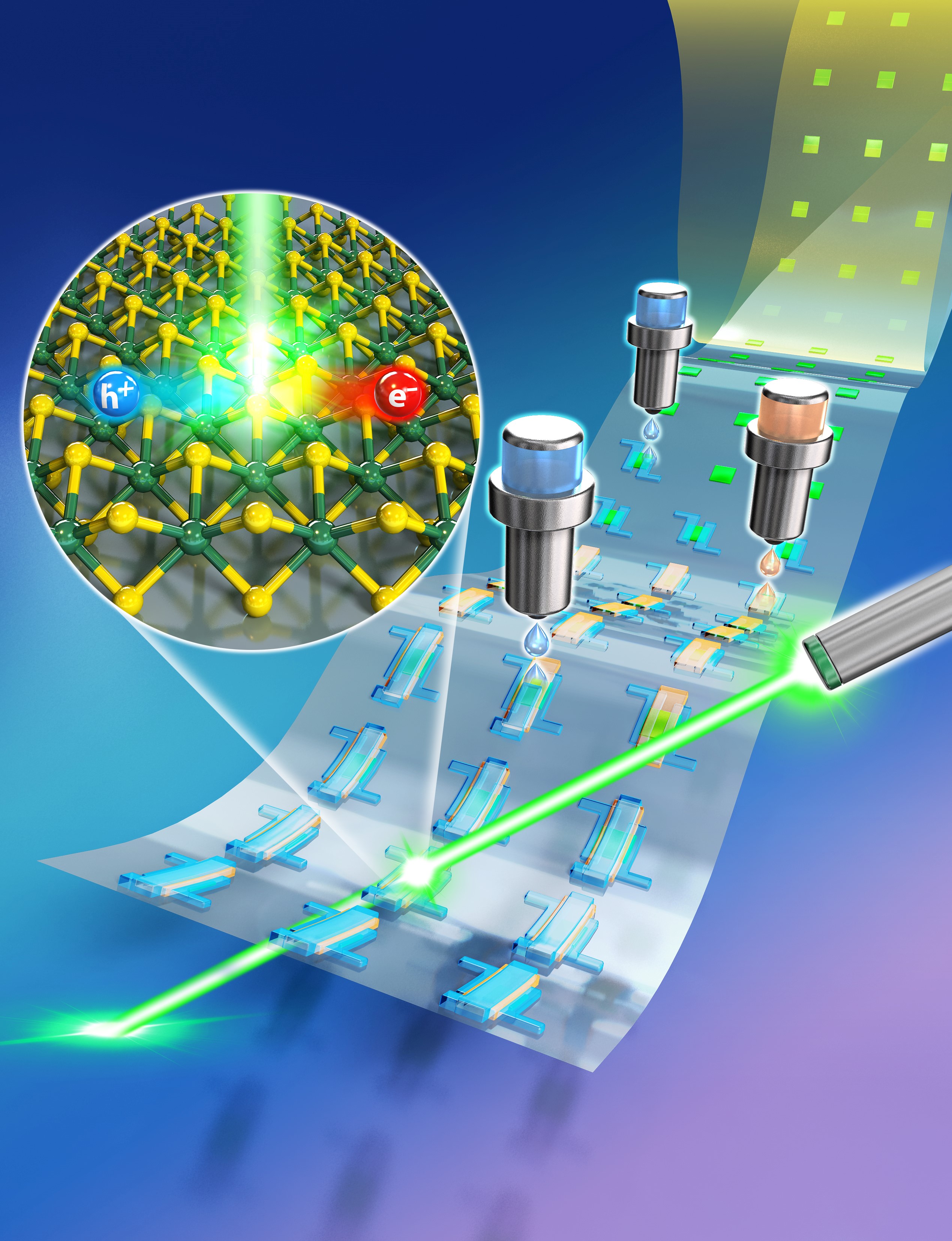
▲MoS2 based phototransistor production process and the schematic diagram of photoreaction
A key technology to advance the development of high-performance transparent optical sensor, which is an essential element of wearable devices, was developed by domestic researchers.
A collaborative research team, which is comprised of Professor Yongtaek Hong of Department of Electrical and Computer Engineering, researcher Jaewook Ha, Professor Takhee Lee of Department of Physics and Astronomy, Professor Seungjune Jung and Dr. Taeyoung Park (Samsung Electronics), succeeded to make flexible large-area transistor array using monolayer MoS2 films.
MoS2 is a next-generation semiconductor material that can be used for flexible electronic devices since it can be made into a single molecule layer and has excellent semiconductor properties such as high charge mobility and flicker ratio. In addition, it can be utilized for various photoelectronic devices such as photodiodes, phototransistors, and optical sensors.
In the past, a top-down method such as mechanical stripping or intercalation was used to obtain a monolayer MoS2. Recently, however, a bottom-up method such as a chemical vapor deposition method, a physical vapor deposition method has been received attention.
Monolayer MoS2 has excellent flexibility and transparency, but in many cases MoS2-based electronic devices use metal electrodes and inorganic insulation layers, making it difficult to fabricate large-size and flexible devices.
To solve this problem, the research team fabricated a transparent and flexible monolayer MoS2 (0.65nm) film in a large area and patterned it into an array. It was transferred onto a plastic substrate, and an electrode and an insulating layer were formed thereon, and a transparent and flexible organic material was formed by inkjet printing, finally succeeded to make MoS2-based phototransistor.
The phototransistor produced by the research team has transparency of over 76% and has a very stable condition, which didn’t show change in characteristics even after repeated bending tests of 1000 times with a radius of 5 mm. Also, as the power of incident light increases, the photoreactivity increases linearly, providing a basis for its use as an optical sensor.
Professor Yongtaek Hong of Department of Electrical and Computer Engineering said, "This research has made it possible to implement a transparent and flexible large-area MoS2-based phototransistor by using the entire printing process. It will become a technical basis that can be applied to large-area and low-cost wearable devices.“
The results of the study was published online on August 25 in ACS Nano, a world-renowned international journal in the field of nanodevices and materials. The study was supported by the Ministry of Science and ICT and Ministry of Trade, Industry and Energy.
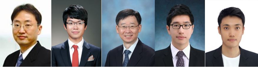
▲ (from the left) Professor Yongtaek Hong, researcher Jaewook Ha, Professor Takhee Lee, Professor Seungjune Jung, Dr. Taeyoung Park (Samsung Electronics)